Through the Frame-Buffer; or, Thomas and Zack’s Adventures in FPGA-Land
It’s a poor sort of memory that only works backwards.
— Lewis Carroll, Through the Looking-Glass and What Alice Found There
Over the past semester, we (Zack Robinson and Thomas Makin) spent a lot of time messing around with a Terasic DE10-Standard board and its onboard Cyclone V FPGA.
Our original end goals were twofold:
- Write Verilog and/or C code to take video frames from an SD card and send them to the board’s VGA output.
- Learn things about FPGA development.
We accomplished Goal 2 with flying colors. Goal 1, on the other hand, was even more difficult than we expected (and we expected it to be difficult). We found minimal, confusing, or nonexistent documentation, 15-minute compile times, weird incompatibilities, and several dozen other random problems, a subset of which are mentioned herein. That said, while we didn’t actually accomplish what we set out to do, we learned a lot in the process. This report is a chronicle of our experience, and we’re publishing it for the Internet with the hope that it can be a helpful resource to anyone trying to follow in our footsteps.
This project, and the report you’re reading now, was the subject of our half-credit directed reading “Further Topics in Computer Architecture” during the Fall 2023 semester at Swarthmore College. It wouldn’t have been possible without the support of Professor Maggie Delano (for teaching us the foundations and agreeing to advise us on rather short notice) and the Swarthmore Engineering Department (for funding a shiny new board for us to work with and for agreeing to give us degree credit for this).
It also seems important to note that we’re the current and former Presidents of the Swarthmore College Computer Society, and did substantially all of our work in the SCCS lounge using an old SCCS monitor for testing. Thank you to SCCS as an institution for existing, and to the other staff members for putting up with our lively debugging sessions.
Prologue
Last semester, we took a course entitled “Principles of Computer Architecture,” in which we learned about the governing properties of modern RISC computer systems and how they work on a hardware level. We learned how to write basic Verilog and MIPS assembly, and as part of the course implemented a single-cycle processor on a simulated DE0-CV development kit. This course ignited our interest in low-level hardware definition platforms, and we decided to get super ambitious for our final project: attempting to play back videos on a VGA display using a Terasic DE0-CV development board.
Unfortunately, this turned out to be WAY out of our wheelhouse with our limited experience, time, documentation, and hardware capability. We instead focused on displaying one image over VGA, which we…mostly succeeded in doing. However, we were not deterred from learning more about how to make this thing tick, so this fall we decided to ask Prof. Delano to be our faculty advisor as we continued our learning for half a credit. Our goals, as outlined above, were to learn more about the Cyclone V FPGA platform (and the toolchains used to write hardware and software for it) and to play back images from an external storage medium.
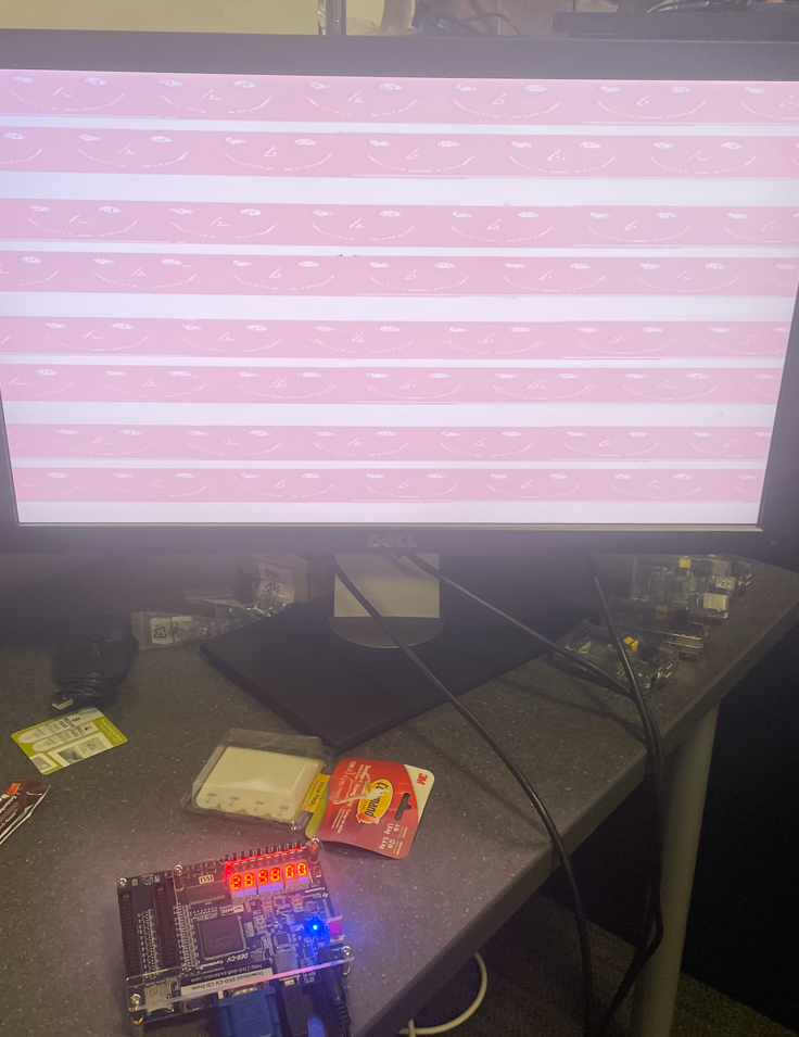
A picture from our first attempt
Part 1: Making Mifs and Memories
Our previous board, the DE0-CV, had some rather unhelpful examples. This new board gave us some cause for optimism: it had better specs and, more importantly, some better examples of how to work with image files. The default out-of-the-box software displays a color image on the VGA output.
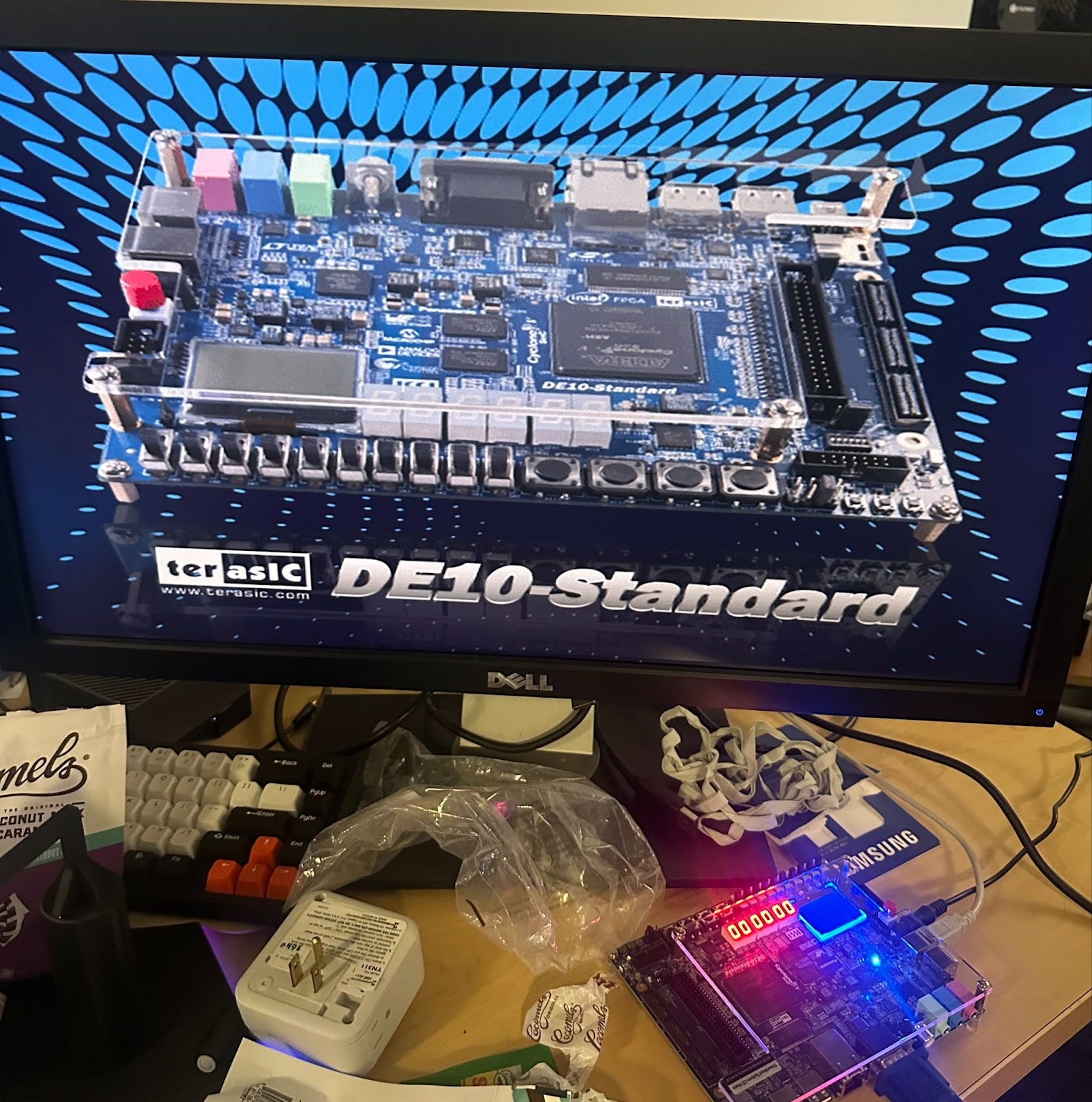
When we looked into the Verilog, we found this in the top-level module:
vga_controller vga_ins(.iRST_n(DLY_RST),
                       .iVGA_CLK(VGA_CTRL_CLK),
                       .oBLANK_n(VGA_BLANK_N),
                       .oHS(VGA_HS),
                       .oVS(VGA_VS),
                       .b_data(VGA_B),
                       .g_data(VGA_G),
                       .r_data(VGA_R));
Pretty simple so far: we’ve got a Verilog module that plugs into a reset line and a clock, and then has several wires for the VGA output: BLANK_N, HS (horizontal sync), VS (vertical sync), B, G, and R.
The precise details of how the VGA protocol works are omitted for brevity (and are easy to find online) but, in short, it sends analog signals on the B, G, and R lines for the blue, green, and red subpixels. One pixel is sent per clock cycle, except for periods at the end of each row and at the end of each column. The HS, VS, and BLANK lines sync the display up so that both the output and the display agree on what pixel is going where. Because it’s a protocol originally developed around the limitations of CRT televisions, it’s also pretty easy to implement in hardware. But when the sync signals are incorrect, or pixel data is out of sync with the clock, you can get tearing, stretching, or other problems (like that image from the prologue). Also, inside the FPGA itself, the B, G, and R values are 10-bit digital values which are later converted into voltages by a simple ADC elsewhere on the board.
Looking into vga_controller.v, we hope to find the code that reads an image from memory and sends it out to the VGA outputs. We’re off to a good start:
always@(posedge iVGA_CLK,negedge iRST_n)
begin
  if (!iRST_n)
     ADDR<=19'd0;
  else if (cHS==1'b0 && cVS==1'b0)
     ADDR<=19'd0;
  else if (cBLANK_n==1'b1)
     ADDR<=ADDR+1;
end
This code resets the address down to zero if the reset line is high (by convention, these examples seem to use a name like iRST_n to mean “input, RST, negated,” so !iRST_n would be True if the original RST line is high). It also resets it if both horizontal and vertical syncs are low, which would imply we’ve made it to the bottom of the image. Otherwise, unless we’re currently on a blank portion of the image (i.e. the front or back porch), it advances the address by one. So far so good.
Now, we find the memory access:
//////INDEX addr.
assign VGA_CLK_n = ~iVGA_CLK;
img_data img_data_inst (
 .address ( ADDR ),
 .clock ( VGA_CLK_n ),
 .q ( index )
 );
//////Color table output
img_index img_index_inst (
 .address ( index ),
 .clock ( iVGA_CLK ),
 .q ( bgr_data_raw)
 );
//////
There are two memory blocks here, which is one more than we expected. To gloss over several hours of consternation, we eventually figured out how this works. The image shown on the screen, in its raw form, is too big to fit in the onboard ROM. 640x480 times three colors, with one byte per color, is 921,600 bytes, too many to fit. Instead of doing that, the people who made this example cut the image down to 256 colors, put each of those colors in an index file, and then loaded in the 640x480 image with one byte per pixel instead — where each byte is an index into the 256-byte index block.
To clarify this, let’s back up and explain how that data got into the ROM in the first place. Quartus has a thing called a Memory Initialization File, or MIF file. When you create a memory block and load a MIF file, then that data is flashed onto the ROM during programming. MIF files are, mercifully, human-readable, which lets us explain by example. The out-of-the-box example comes with two MIF files: index_logo.mif and img_data_logo.mif. index_logo.mif looks (in part) like this:
WIDTH = 24;
DEPTH = 256;

ADDRESS_RADIX = HEX;
DATA_RADIX = HEX;

CONTENT BEGIN
0:fc9d1e;
1:33010d;
2:abaab5;
3:5d4bf9;
4:280ebb;
5:8674e9;
[SNIP]
fb:0b0c15;
fc:292a36;
fd:878896;
fe:fcfcfc;
ff:ffffff;
END;
This defines a memory block with 256 24-bit-wide memory entries. The color data at index 0, for example, is fc9d1e, which is a nice light-blue color. (The color is ordered as B, G, R, which is the opposite of web hex codes. That color is actually #1e9dfc on the Internet.)
Now let’s look at the actual image data in img_data_logo.mif:
WIDTH = 8;
DEPTH = 307200;

ADDRESS_RADIX = HEX;
DATA_RADIX = HEX;

CONTENT BEGIN
0:01;
1:01;
2:01;
3:01;
4:01;
5:01;
[etc]
This continues for about 300,000 more lines. Note, however, that it’s only 8 bits wide, and 307200 words deep. And pixels 0 through 5 in the image all have the data 01, which — if we go back up to the index file — corresponds to the actual color data 33010d.
It wouldn’t be terribly hard to write a bit of software to generate these files ourselves, but luckily, Terasic ships these boards with a program: PrintNum.exe. This takes a bitmap file and converts it to two MIF files. Except that it doesn’t, because the program doesn’t add the necessary header lines (all that stuff before CONTENT BEGIN). We had to write another PowerShell wrapper to do that.
After getting the PowerShell wrapper working, we were able to load arbitrary bitmaps into the ROM and display them on the screen:
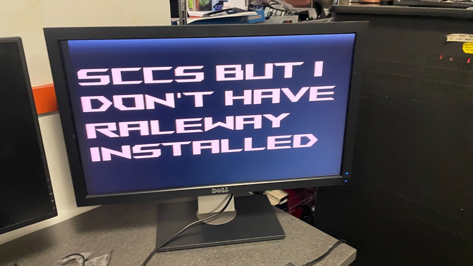
Context: we wanted to display the SCCS logo but Thomas didn’t have the font installed on his local computer.
At this point we were back to where we had left off last semester, except on a nicer board and we understood everything a lot better.
However, we were only reading images out of ROM at this point. Our next step was to read something out of RAM. The thinking was if we were able to read arbitrary images from RAM, then we could separately figure out how to write whatever we wanted into RAM and have it display on the screen.
Part 2: Downloading Software is Hard
The example projects and most FPGA designs in general include IP blocks, or prewritten, obfuscated, DRM’d implementations of different components such as SDRAM readers, VGA clock generators, and the like. Unfortunately, they are subject to license restrictions, which vary by device and component. When we attempted to open some of the example code for the DE10-Standard in newer versions of Quartus, we noticed that it refused to let us use the SDRAM controller. As it turns out, after Quartus 16.1, Intel/Altera made that component available to subscribers only. Given that we weren’t going to pay thousands of dollars for a Quartus Pro license, we went to work finding a download link for Quartus Lite 16.1.
Searching through Intel’s FPGA Software Download Center, we discovered that while there were download links for Quartus 13.1 and 19.1, there was nothing in between. A quick search revealed they had nuked the download links, but in theory the original links still worked…if we could figure out the URL scheme.
After a bunch of Googling, we found quartus-install.py from GitHub user CTSRD-CHERI, which was a scripted downloader for various Quartus versions. Since it was intended for servers, it only downloaded the Linux versions, but it had a download link for Quartus 16.1. On a hunch, we changed linux.run to windows.exe at the end of the URL and managed to download Quartus 16.1 for Windows. We were now able to compile and run SDRAM testing examples.
Part 3: The Nios II Toolchain
The DE10 came with two SDRAM testing examples: one in straight Verilog, very similar to the one that we used previously, and one using the Nios II processor. The Verilog example is, like the one we found last semester, not really an example: the WRITE_ADDR line isn’t even wired up. The Nios II example, on the other hand, was much nicer, and let us move a little bit higher on the abstraction stack.
The Nios II is a “soft core:” an entire industrial-grade (ish) central processing unit implemented completely within the FPGA. You drop it in just like any other module. The examples using the Nios, however, are not handwritten Verilog: instead, they use Qsys, which is a graphical system integration tool that lets you define modules at a higher level and plug them into each other much more easily.
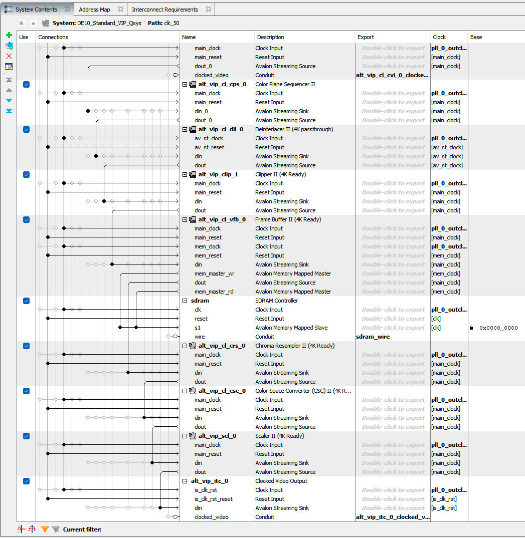
An example Qsys design.
The Nios uses the Avalon memory-mapped interface to communicate with other parts of the FPGA design (more on that later), with the JTAG debug interface for talking to the development computer. We found it fairly easy to compile and deploy the hardware design onto the FPGA (Qsys generates Verilog files which you compile using the standard Quartus compilation process); software was another story.
In Windows-host development, toolchains generally follow one of two routes: have an enormous stack of dependencies and use native compilation (usually depending on ~15 GB of garbage from Visual Studio Build tools), or give up and just use Linux (via MSYS/mingw, cygwin, or WSL). While Quartus itself uses its own toolchain and therefore does not need either (it comes with its own many-gigabyte compilation suite), the Nios II toolchain is gcc-based and uses the second strategy.
It would appear the developers at Altera/Intel and Terasic were unable to decide whether they wanted to use cygwin or WSL, so they took a compromising approach: use both. The Nios II Software Build Tools Command Line is a cygwin-based terminal where you run WSL-based scripts. The Nios II developer on a Windows machine must use cmd to run the batch file that opens said SBT command line, followed by cygwin to execute scripts, often followed by WSL to perform logic. This is a pain to deal with as is, but because the example code is completely unmaintained, the scripts included (and some Nios toolchain scripts) will not run on the latest versions of WSL without modifications–specifically, their hardcoded uname check to ensure it was running in WSL. The scripts checked for Microsoft in the kernel string (which was the case in WSL1 it seems, see 2.1. Windows* Subsystem for Linux* (WSL 1) on Windows Requirements…) instead of microsoft. You’d think they would have at least made it a regex. We were unsure of why things weren’t working even when we ran the scripts manually until we discovered the wslenv hackery they crammed in to ensure commands could be run in their cobbled-together environment.
As it turns out, the proper startup flow (or at least what worked for us) was to patch scripts with the kernel string check and utilize the ./create-this-app script to initialize an example project. For subsequent builds we would generate the BSP (Board Support Package) files using the nios2-bsp-generate-files command (run once per Quartus compile as the BSP updates to match your components), followed by make download-elf (run once per code change) to compile the program and start it on the processor.
Part 4: Inside Of You There Are Two Video IP Cores
After fixing the toolchain, we got the premade example — SDRAM testing with Nios — running properly on the Nios processor within the FPGA. Running nios2-terminal -c 1 let us open up a serial console and see print output, which was helpful for debugging and let us see that it was in fact writing to the RAM.
We also looked through the examples for the Altera/Intel Video and Image Processing Suite (VIPS), which is a set of prebuilt IP cores for processing video using the Avalon streaming protocol. This lets us plug what are essentially prebuilt pipeline stages into each other pretty easily. We still spent a long time trying to figure out why things weren’t working, but it wasn’t about connections: mostly just misclicks that applied configuration changes we didn’t realize, along with extremely odd naming conventions.
The nice thing about these cores is that Qsys is actually very smart about them. Since the VIPS can handle a wide variety of different kinds of video streams, it’s very easy to accidentally configure one part of the chain to e.g. work with a 1920x1080 stream of 12-bit color when the rest of your pipeline is 640x480 with 24-bit color. Qsys will catch this and emit an error at the connection point. Of course, just like most programming environments, it can’t catch when you told it to do something even though you actually wanted to do something else. For example, the Nios II example and the video streaming example had their clocks configured differently, which we didn’t catch for a while and which caused the video side of things to simply not work. (The Nios II can run at various frequencies, but VGA, being a timed protocol, has to be pushing pixels at a very specific 25 MHz rate.)
There was one point of confusion, though: in Qsys, we found two almost-identical sets of video IP cores. “Frame Buffer” and “Frame Buffer II (4K Ready),” “Clocked Video Output” and “Clocked Video Output II (4K Ready),” and so on. We’re still not actually sure what the difference between these two sets of cores are (although we found diverging documentation that seems to indicate that they have different control registers), but all we know is that nothing works when using the first set, and we needed to use the second set (“4K Ready”) to get anything at all to show up on the screen. After we figured that out, though, we were able to use a Test Pattern Generator (4K Ready) plugged into a Clocked Video Output (4K Ready), that we then wired to the VGA output lines on the FPGA. This correctly displayed a test pattern on the screen:
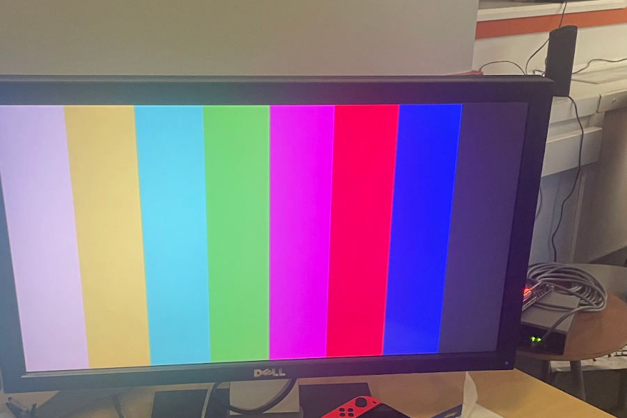
A test pattern!
We then took this same setup of a test pattern feeding into a clocked video output and put it at the bottom of the Nios II example project. After some further issues (we had set another clock frequency wrong and hadn’t realized it, and there were several naming issues), we managed to get the test pattern running alongside the SDRAM test in the same FPGA design.
Part 5: What The €š�舐 Is An Avalon Memory Mapped Interface?
The next step was to figure out how to get the Nios II processor (and by extension, the C code running onboard) to talk to the video cores. Our Nios + SDRAM example was very helpful here, containing several examples of how to talk to the SDRAM IP core over the Avalon Memory-Mapped Interface (Avalon-MM). We also found a guide to Qsys Interconnect hosted on a Cornell ECE website, which was very helpful to understand the contours of the general system, and a comprehensive specification hosted on a Columbia CS website.
Basically, Avalon-MM lets us treat each IP core as a small block of memory. (Or, in the case of the SDRAM, a large block of memory.) Reads and writes to this memory let us read status from, and issue commands to, various IP blocks.
For example, the parallel IO component lets us interface with arbitrary digital logic inputs (in our case, the four physical push buttons on the board). When placed into Qsys, it exports wires that can be wired up to the board inputs (using Verilog). It also exposes an Avalon memory-mapped slave which can be connected to the Nios core and read from to read the state of the buttons. The specific memory address is set in Quartus: every master (such as a processor, or a framebuffer component) can have independent address mappings for each slave it is connected to. Something which is non-obvious, but makes some sense, is that there can be a many-to-many relationship between masters and slaves: you can have as many masters as you like connected to the same slave. Qsys will even add the necessary circuitry in order to properly sequence read and write operations. That said, it’s possible that we missed something there, because our attempts to write to the same SDRAM buffer that our frame reader was reading from never actually worked.
The PIO IP core was named key in QSYS, and so reading from the button value is as simple as:
ButtonStatus = IORD(KEY_BASE, 0);
on the embedded processor. Here, KEY_BASE is a value from system.h, a file that’s automatically generated as part of the BSP from the memory mappings set in Qsys. The n-th bit of this ButtonStatus value is the status (high or low) of the n-th input to the IP core. This is from the example code for reading and writing to memory, which waits for a button to be pressed, then runs the memory test. Zooming out, we can see how the example code does this waiting:
while((ButtonStatus & ButtonMask) == ButtonMask){
  ButtonStatus = IORD(KEY_BASE, 0);
}
Our next experiment was to attempt to control a Switch component in order to change the display output between two different test patterns. We put the Switch II component into Qsys, and wired up a color test pattern to one input and a black-and-white test pattern to the other input, then wired the output to the clocked video output that we had been using earlier. Finally, it has a “memory mapped slave” input port that we wired to the Nios II data master and set an address range appropriately in Qsys. (We just took the highest address value that we had allocated already and added 1.)
The documentation specifies several control registers that we needed to hit from the Nios processor. Registers 0, 1, and 2 are standardized across all the VIPS IP cores, while the remainder are core-specific:
- Word 0 of the memory block is the
Controlregister, which lets us turn the entire core on or off. - Word 1 is the
Statusregister, which we can read from to get the on-or-off status of the core. (It might take a few clock cycles forControlto go into effect, so this is useful to wait until the core is running properly.) - Word 2 is the
Interruptregister, which in this core, is used to signal that a switching operation is complete. - Word 3 is the
Output Switchregister, which we can write to to signal to the component that it should check the switching registers and synchronize its output streams. - Words 4–15 are output control registers. (We only used word 4, because we only had one output.) To route input n to our output, we needed to set the n-th bit to 1 and all other bits to zero.
Our first quick-and-dirty task was to check if writing to Control even worked. So we replaced the SDRAM testing code with:
int control = IORD(SWITCH_BASE, 0);
int status;
while(1) {
  status = IORD(SWITCH_BASE, 1);
  if (control == status) {
    control = status ? 0 : 1;
    printf("Setting status to %d\n", status);
    IOWR(SWITCH_BASE, 0, control);
  }
}
This code reads the switch’s Status register, then tells the switch to shut off or turn back on (whatever the opposite of its current state is) using the Control register. This promptly spammed our terminal with alternating Setting status to 0 and Setting status to 1 messages, which was exactly what we expected to happen!
We then tried to actually use the switch, in conjunction with the buttons, to switch video streams. This was much easier to get working, because we could recompile and redeploy the code in under 15 seconds instead of 15 minutes.
while (1) {
  ButtonStatus = 0;
  // wait for button press
  while (!ButtonStatus) {
    ButtonStatus = ~IORD(KEY_BASE, 0) & ButtonMask;
  }

  printf("Writing %d to switch reg", ButtonStatus);
  IOWR(SWITCH_BASE, 4, ButtonStatus);
  IOWR(SWITCH_BASE, 3, 1); // output switch

  // wait for button release
  while (ButtonStatus) {
    ButtonStatus = ~IORD(KEY_BASE, 0) & ButtonMask;
  }
}
Note that the parallel port reads a button being pushed as 0, e.g. only button 1 being pushed will result in a signal of 0b1101. So, we invert the signal before masking off the buttons that we want to read. (ButtonMask is 0xF here, for masking the first four bits of the register.)
And it actually worked!
Our next step was to use the Frame Buffer II component to try to read and/or write frames from memory. If we can read arbitrary frames out of memory, then it shouldn’t be too hard to put arbitrary frames into memory. But it turns out that that was hard.
The frame buffer component has three modes: Frame Writer (just puts frames in RAM), Frame Reader (just reads frames from RAM), and buffer (both writes and reads). We first tried to put the frame buffer component in the middle of the video stream, just to see it work. When in buffer mode, the buffer takes a video input, talks to the SDRAM controller to store the frames, and then outputs buffered frames on its video output line. This worked fine.
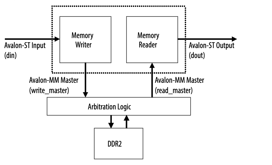
Credit: Frame Buffer II Documentation
We then tried to put the frame buffer in Frame Reader mode, where it would read from whatever blocks of SDRAM we told it to read from. As a test, in lieu of writing a bunch of code to write an actual image to RAM, we instead used the psuedo-random data that had already been written by the memory test routine.
The docs had a helpful page on exactly what we would need to do to get this reader working. The frame reader core sets the Ready bit (bit 26 of register 7) whenever it’s ready to accept information on a new frame. Then, it expects the width and height of the frame to be written into the Frame Information register, followed by the actual start address of the frame in RAM written into the Frame Start Address register.
We wrote the C code to implement this protocol, and at this point, the frame buffer was supposed to start transmitting frames. But, as far as we could tell, it didn’t. It also only ever accepted one frame: the Ready bit would never go high again after we wrote the frame information once. And we didn’t get any video output. We tried all sorts of different experiments to see if we could make it work: incrementing the frame address that we wrote, setting and resetting the Control registers to turn it off and back on again before running, even writing a simple HAL library to try and rule out stupid typos in our register numbers.
To make matters worse, running the frame reader seemed to start causing weird memory corruption gremlins in our code. Even after removing frame-reader-related code, we’d start to see output like
Starting frame reader
Waiting for frame reader to be ready
Frame reader is€š�舐
These memory gremlins would continue even through code re-deploys, up until we would have to power cycle the FPGA and completely re-write the design back to the chip. We’re still not sure what actually caused this, because the Nios II is supposed to be storing all of its stack data in on-chip memory, and the frame reader should not be writing to any memory so enabling it really shouldn’t do anything. It’s entirely possible that we missed something very obvious here, but we spent quite a lot of time poking around and were totally unable to get past this.
We also found an example that seemed to have something exactly like what we wanted to do (it displayed a generated “radar screen” image using a frame reader). We tried to look through the code, and as far as we can tell, it didn’t do anything differently than we were doing; that said, it was wrapped in quite a lot of object-oriented library stuff.
At this point, we were pretty much at a loss. We could potentially have tried to rework our memory layout, or rewritten everything from scratch, or tried every possible combination of parameters on the frame reader to see if it helped. Instead, though, we thought we might learn a bit more by trying to debug our system using some external tools.
Part 6: We Found The Debug Panel
Part of the point of designing systems for an FPGA platform is ease of debugging. The USB interface on the board supports JTAG, which is a (somewhat) standard protocol for debugging systems and software and the earliest stages of bringup. JTAG stands for Joint Test Action Group, which is the group that founded the “standard” (it varies substantially for different architectures, adapters, boards, and platforms, so to call it a “standard” is somewhat misleading — note the many conditionals on the Wikipedia page such as “The TRST pin is an optional active-low reset to the test logic, usually asynchronous, but sometimes synchronous, depending on the chip.”). JTAG is a complex protocol and transmits different kinds of data differently, so Altera/Intel has set up QSYS to hide extra fabrics in the backend that make adding JTAG-based trace systems way easier. For the Video Image Processing suite, the recommended setup is to use an Avalon-ST Video Monitor, which takes samples of passing frames on an Avalon-ST streaming bus, and connect it to a Trace System IP core, which is a more generic component that exposes traceable components over JTAG via the System Console.
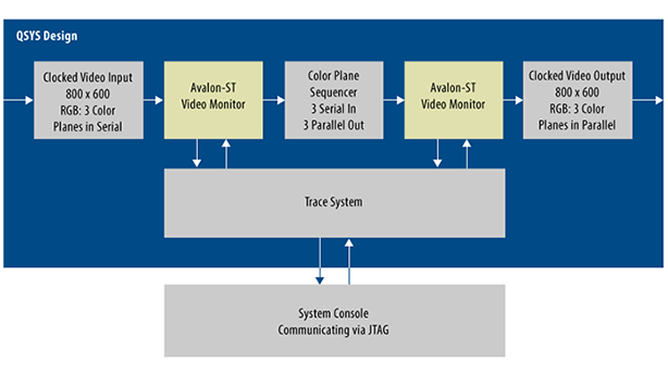
While attempting to initialize the Frame Buffer II IP core in various ways, this system was extremely helpful because it allowed us to see not only what the VGA output showed, but also the frames in transit at various stages. To set up this system, we placed an Avalon-ST Video Monitor between our Test Pattern Generator and our Frame Buffer, and hooked up a Trace System. These systems are configured in the System Console, where we set parameters (trace system to collect from, types of data collected, and capture rate) and start/stop packet capture. For each transmitted frame, there are two discrete packets sent: video control and video data. The control packet contains metadata about and parameters passed with the stream, whereas the data packet contains the frame data itself. System Console can reconstruct an image from sampling this data (hence needing to tune the sample rate). We found that a capture rate of ~2500 per 1000000 pixels worked well, as sampling too high caused underrun and sampling too low made the picture useless.
Epilogue and Postmortem
The overarching themes of this project, along with our other forays into the world of FPGAs, is that this platform is meant for graduate students and enterprise customers. Want better documentation? Want better examples? Want to use the newer version of Quartus? Want to make iterative compilation not suck up hours of time? Buy our subscription. We did not have this subscription and had to depend mostly on incomplete examples from Terasic (which were at least way better than the DE0-CV examples), raw datasheets from Intel, guessed link migrations from Altera’s wiki to Intel’s, and random examples we found online from advanced engineering courses at large research institutions.
This is not to say that we made no progress or that we didn’t enjoy this work–this was a very fun, interesting, and intellectually stimulating project that we were heavily motivated to keep working on. We have hundreds of pages of messages between us where we found more and more pieces of the puzzle. Our understanding of how these systems work on a fundamental level has progressed far beyond what we expected going in, from the higher-level system layout done in Qsys to the hardware initialization done on the processor. The amount of celebration in the SCCS lounge when a frame would finally appear on the screen was borderline cultish.
We do wish we could have finished what we started (and continued beyond our original vision as well) but the amount of work required ended up being beyond what we expected. We learned a lot and we wrote a ton of code and we displayed a ton of frames. We are proud of the progress we have made and hope this report and any future addendums to this project we may make independently can serve as open documentation for people of our entry level.
Thanks for reading!